
Calculation of Power Supply RC Snubber Values from Measured Circuit Parasitics
Published by Hilbrand Sybesma, Principal Hardware Engineer at E3 Compliance
With the many switching circuits around, it is common to see ringing in the switching node which many times leads to electronic equipment not complying with EMC requirements. There are many articles written on designing a snubber to damp out the ringing, but after starting the analysis with mathematics for defining the existing circuit component values, they then turn to fuzzy guesses in selecting the Snubber Resistor and Capacitor values. This article is a complete mathematical analysis for both determining the parasitics and calculating snubber resistor and capacitor values.
In the following figures 1 and 2 you can see where an LTSpice simulator predicts there will be ringing on node Vsw2 in this SEPIC SMPS. The prediction was correct, but the frequency and damping ratio were slightly different in the actual circuit. This is because the simulation does not include all PCB circuit parasitics of the components and layout. In the case of this circuit, it was necessary to eliminate the ringing.

This ringing is caused by parasitic inductance (primarily the circuit inductor), parasitic capacitance and parasitic resistance, all forming a simple RLC circuit. The frequency of the oscillation is caused by L and C while the decay is dependent on R and L.
Figure 3 shows how the circuit is modeled with R1, L1 and C1 being the parasitic components while R2 and C2 represent the snubber components. The input supply V1 provides the driving square wave. Before getting to determining the parasitics, we will first perform some analysis to see how these components interact.

We start by developing the nodal equations needed to solve the circuit and then solve.
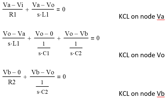
Of interest is "H(s) = Vo(s) / Vi(s)". The transfer function comprises one Zero and three Poles. As typical for system analysis, we are most interested in the characteristic equation of the denominator, but it is necessary to understand what the transfer function is telling us about how the snubber components affect the circuit.

To understand how R2 and C2 will affect the response, let's look at four conditions: When R2 approaches zero, when R2 approaches infinity, when C2 approaches zero and when C2 approaches infinity.

Four things should be taken from these results:
Eq1 shows that as R2-->∞, the basic characteristic equation is achieved that has both R2 and C2 removed and having no effect. This indicates that there is some maximum value for R2 above which there is vanishing effect. This result will be used in determining the value of R1.
Eq2 shows that as C2-->0, the basic characteristic equation is achieved that has both R2 and C2 removed and having no effect. This indicates that there is some minimum value for C2 below which there is vanishing effect.
Eq3 shows that as R2-->0, the characteristic equation changes such that the natural frequency is now dependent on the sum of the two capacitors, C1 and C2, multiplied by L1. This result, and Eq2, will be used in determining the values of C1 and L1.
Eq4 shows that as C2-->∞, the characteristic equation changes to where the ratio of R2 and R1 now have influence over both the natural frequency and damping. This effect is important in determining a value for R2.
Determine L1, C1, R1 Parasitic Values:
To determine these values, three (3) measurements must be made.
Measure the frequency of the ringing of the unmodified circuit. This will be frequency F1.
Measure the peaks during the decay on the unmodified circuit for both value and time along with its steady state DC offset. This decay information will be used to determine R1.
Add capacitor C2 with R2=0. This is per Eq3 above. Be sure to measure C2 and not use its rated value. The act of soldering can also change its value so confirm afterwards also. You want to select a value so the frequency will change significantly, cutting it in half or third for a better reading. This will be frequency F2. The value will normally be small (100pF to 2nF).
With the two frequencies, F1 and F2, their natural frequencies are defined as follows: These relationships, from Eq1/Eq2 and Eq3 above, are used to first solve for C1 and then using C1 to solve for L1.

Using the measured frequencies and value of C2 when generating F2, the parasitic capacitance is:

Knowing C1, the relationship can be solved for the parasitic inductance L1:

The parasitic resistance can be determined from the decay envelope. Using the peak values and peak times, the decay envelope can be defined and R1 determined. Using characteristic equation from Eq1, α is defined.

The decay envelope formula is defined as:

Substituting, R1 would be as follows. You should calculate R1 using several peaks and determine an average.

Measurements from the above two graphs, on the SEPIC converter, resulted in the following:

Now the parasitics are known and can be put in a circuit simulator to confirm what was observed. At this point there are two options for determining values for the snubber resistor and capacitor.
Iterative. Determine the snubber values in a circuit simulator using the iterative method. This involves changing the snubber component values, observing the resulting waveform and power dissipation in R2. Using this method requires keeping in mind that a little overshoot is not the same thing as ringing. This is easily verified by putting the component values selected in the characteristic equation and determining the roots to ensure all three are real.
Analytical. Continue the mathematical circuit analysis. This involves further use of equations Eq0, Eq3 and Eq4. Solving a characteristic equation for R2 and solving a discriminate for C2.
Calculate C2, R2 Snubber Values:
R2 can now be calculated using the characteristic equation from Eq4. Being a simple 2nd order polynomial, the solution is straightforward.

Now use the above relationship for critical damping and symbolically solve for R2. Using the parasitic values determined above, the value for R2 is:

Given that only a positive real value for R2 is desired, the value will be:

It is important here to point out that this value of R2 is a maximum value determined assuming an infinite value of C2. So, when the value of R2 is 372Ω, with an infinite value for C2 (or shorted), the circuit is critically damped. Smaller values will be over damped and larger values will be under damped.
A Root Locus can also be generated to track the motion of the roots as R2 is changed. When R2 is small, the roots are real and far apart on x-axis (over damped) with increased losses. As R2 increases they come closer together, meeting (critical damping), and then splitting in complex conjugate pairs (under damped). The more under damped they become, the more overshoot and ringing will be increased looking more like having no snubber. Figure 4 below was generated using a C2 value of 2.2mF and R2 ranging from 50Ω to 1000Ω. Critical damping for R2 is about 372Ω.

All values for the characteristic equation are now known except C2. Being a polynomial of degree three makes solving for C2 symbolically very difficult. However, since we wish to solve for a value that provides critical damping, an alternative method is available. The form for a 3rd order polynomial is given as:

Its discriminate is then given as:

where, if all coefficients are real:
if Δ 3 > 0, then equation has three distinct roots
if Δ 3 = 0, then equation has repeated roots and all roots are real
if Δ 3 < 0, then there is one real root and two complex conjugate roots
We wish to solve for C2 where Δ3 = 0 as this will be the point of critical damping where there are repeated roots - the point between separating into two distinct real roots or two complex conjugate roots. Since solving symbolically for C2 is difficult, instead use the known values to calculate the coefficients with C2 being the only variable.
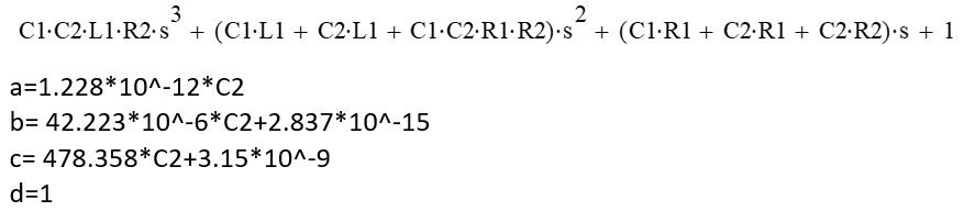
At this point you will need to use your favorite Math application and enter the coefficients a, b, c and d into the discriminate, set it equal to 0 and solve for C2. Using the values already determined for L1, C1, R1 and R2 will result in the following solution.

Given that only a positive real value for C2 is desired, its value at critical damping will be 888pF. This is the minimum value for C2.

Figure 5 shows the Root Locus for C2 from 50pF to 2nF with R2=372Ω. Critical damping occurs at about 890pF.

Since there are more values of resistors than capacitors, you may wish to now select a next larger standard value for C2 and calculate a value for R2. This is accomplished simply by repeating the above calculation using the discriminate but instead solve for R2.
If, for example, C2 was selected as 1nF, then (in this example) critical damping will occur with two different real values for R2. One would be 349.7Ω and the other at 426.4Ω as shown here.

To understand what this means, another Root Locus is plotted in Figure 6, this time with C2=1nF and R2 ranging from 200Ω to 800Ω. At 200Ω there are two complex conjugate roots (underdamped) on the right and one real root way off to the left. As the value of R2 is increased, the poles on the right head toward the real axis and meet at R2=350Ω (critical damping). Further increases to R2 cause the poles to split into two separate real roots, one headed out to the left and the other toward the right, chasing the zero of the numerator. There are now three real roots (overdamped). When R2=426Ω, the two poles on the left meet to create a second critical damping point. Further increases to R2 will then cause these two roots to become complex conjugates (under damped).

The engineer searching for one solution for critical damping now has two. The larger value of 426Ω will provide the faster response at critical damping as the poles are farthest away from the origin and one pole is close to the zero to reduce its effect. This will have the lowest over-shoot and the least power loss at critical damping. Figure 7 shows the step response for R2 values of 200Ω, 350Ω, 426Ω and 800Ω corresponding to the four points indicated in Figure 6. At 200Ω there is 21.1% over-shoot, lower frequency ringing and significant slewing. At 350Ω there is 10.6% over-shoot, no ringing and good slewing. At 426Ω there is 8% over-shoot, no ringing and slightly faster slewing. At 800Ω there is 16.2% overshoot, faster ringing and faster slewing.

For completeness, figure 8 shows the actual circuit measurement again, under light load, with no snubber circuit, which shows the underdamped oscillation, and figure 9 which shows the damped oscillation using measured snubber component values of C2=1.07nF and R2=472Ω (components available in the parts bin). This provides empirical data supporting the mathematical analysis.

The above analysis shows how to measure parasitic circuit parameters that cause ringing in the switching node and how to use these values to then calculate exact R and C snubber component values to achieve critical damping. From this point an engineering decision can be made on changes to the damping to meet Voltage, Power and EMI requirements.